
Home page of Parallel Processing
Ελληνική έκδοση (Greek version)
Sorting on a Linear array
1) Theoretical description of the algorithm
We have a linear array with Ν processing elements. We make the decision that the data input and output takes place in each processing element (for other types of input-output there are other algorithms).
We suppose that N is even. The MCUs are enumerated from 1 to N. The operation is split into 2 (two) parts.
- At the first part, the odd MCUs compare their data with the data of the MCU that lies on their right (MCU1 with MCU2, MCU3 with MCU4, and so on). If the data are not in the correct order they are exchanged.
- At the second part, the even MCUs compare and exchange their data with the MCUs that are on their right (MCU3 with MCU4, and so on).
The hole procedure is repeated N/2 times.
The next figure shows this procedure (for N=8).
More details about the correctness and the efficiency of the algorithm can be found in the book of F.T.Leighton.
The implementation of the algorithm is done with 8 (eight) Processing Elements.
2) Interconnection network and I/O
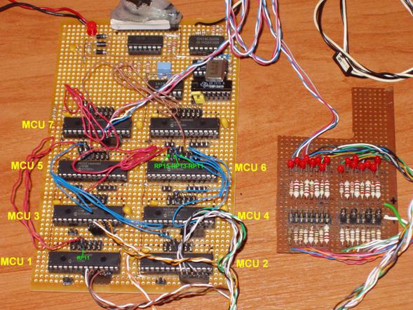
The implementation takes place on the "Parallel PIC" (Revision 1.0).
Each processing element must read the data from some free port. At the specific example the input is only 2 (two) bits wide and uses PortA(0,1). The output is placed on PortA(3,4).
Each MCU uses 1 (one) UART. the transmitter is mapped into RP15 to communicate with the left MCU, and into RP13 to communicate with the right MCU. The receiver is mapped into RP14 to communicate with the left MCU and into RP12 to communicate with the right MCU. The interconnection network is constructed connecting the RP13 of each MCU with the RP14 of its right MCU, and the RP12 of each MCU with the RP15 of its right MCU. MCU1 has RP15 unconnected, and MCU8 has its RP13 unconnected.
One photograph with the board (Revision 1.0) can be found here. The second board on the right supplies the 8 input signals (2-bits each) and displays the output signals (2 bits each).
3) Pseudo-code implementation
Each of the two parts described in the theoretical description is split into 2 (two) steps: one for the "odd" processing elements (1,3,5,7) and one for the "even" processing elements (2,4,6,8). At the second part of the algorithm, the first (1) and the last (N) processing elements are not used, so they must be in "controlled inactiveness", that is they must wait until the the other processing elements finish the second part. In conclusion, there are 4 (four) versions of the basic code. We give them the names: Odd_left, Odd_Middle, Even_Middle, Even_Right.
The pseudo-code follows:
|
W1 <-- read_data for i = 1 to 4 // first phase // if (even) then SEND(left) <-- W1 if (odd) then W2 <-- RECEIVE(right) if (odd) then if W1 < W2 then swap(W1,W2) endif if (odd) then SEND(right) <-- W2 if (even) then W1 <-- RECEIVE(left)
//second phase // if (odd & not leftmost) then SEND(left) <-- W1 if (even & not rightmost) then W2 <-- RECEIVE(right) if (even & not rightmost) then if W1 < W2 then swap(W1,W2) endif if (even & not rightmost) then SEND(right) <-- W2 if (odd & not leftmost) then W1 <-- RECEIVE(left) next i Write_data(W1) |
4) Code
The code follows:
;Odd_L ;================= ; read value MOV PORTA,W1 AND W1,W4,W1 ;================= ; Set counter MOV #4,W7 ;================= loop: setup_RxD_RP12 ;================= ; send data NOP ;================= wait ;================= ; receive data MOV U1RXREG,W2 ;================= ; compare-exchange CP W1,W2 BRA LE,labA MOV W1,W3 MOV W2,W1 MOV W3,W2 BRA labB labA: NOP NOP NOP NOP labB : ;================= ; send data MOV W2,U1TXREG ;================= wait ;================= ; receive data NOP ;================= NOP NOP NOP NOP NOP NOP NOP NOP ;================= ; send data NOP ;================= wait ;================= ; receive data NOP ;================= ; compare-exchange NOP NOP NOP NOP NOP NOP NOP ;================= ; send data NOP ;================= wait ;================= ; receive data NOP ;================= DEC W7,W7 BRA NZ,loop ;================= ; Write value AND W1,W4,W1 SL W1,#3,W1 MOV W1,PORTA |
;Even_M ;================= ; read value MOV PORTA,W1 AND W1,W4,W1 ;================= ; Set counter MOV #4,W7 ;================= loop: setup_RxD_RP14 ;================= ; send data MOV W1,U1TXREG ;================= wait ;================= ; receive data NOP ;================= ; compare-exchange NOP NOP NOP NOP NOP NOP NOP ;================= ; send data NOP ;================= wait ;================= ; receive data MOV U1RXREG,W1 ;================= setup_RxD_RP12 ;================= ; send data NOP ;================= wait ;================= ; receive data MOV U1RXREG,W2 ;================= ; compare-exchange CP W1,W2 BRA LE,labA MOV W1,W3 MOV W2,W1 MOV W3,W2 BRA labB labA: NOP NOP NOP NOP labB : ;================= ; send data MOV W2,U1TXREG ;================= wait ;================= ; receive data NOP ;================= DEC W7,W7 BRA NZ,loop ;================= ; Write value AND W1,W4,W1 SL W1,#3,W1 MOV W1,PORTA |
;Odd_M ;================= ; read value MOV PORTA,W1 AND W1,W4,W1 ;================= ; Set counter MOV #4,W7 ;================= loop: setup_RxD_RP12 ;================= ; send data NOP ;================= wait ;================= ; receive data MOV U1RXREG,W2 ;================= ; compare-exchange CP W1,W2 BRA LE,labA MOV W1,W3 MOV W2,W1 MOV W3,W2 BRA labB labA: NOP NOP NOP NOP labB : ;================= ; send data MOV W2,U1TXREG ;================= wait ;================= ; receive data NOP ;================= setup_RxD_RP14 ;================= ; send data MOV W1,U1TXREG ;================= wait ;================= ; receive data NOP ;================= ; compare-exchange NOP NOP NOP NOP NOP NOP NOP ;================= ; send data NOP ;================= wait ;================= ; receive data MOV U1RXREG,W1 ;================= DEC W7,W7 BRA NZ,loop ;================= ; Write value AND W1,W4,W1 SL W1,#3,W1 MOV W1,PORTA |
;Even_R ;================= ; read value MOV PORTA,W1 AND W1,W4,W1 ;================= ; Set counter MOV #4,W7 ;================= loop: setup_RxD_RP14 ;================= ; send data MOV W1,U1TXREG ;================= wait ;================= ; receive data NOP ;================= ; compare-exchange NOP NOP NOP NOP NOP NOP NOP ;================= ; send data NOP ;================= wait ;================= ; receive data MOV U1RXREG,W1 ;================= NOP NOP NOP NOP NOP NOP NOP NOP ;================= ; send data NOP ;================= wait ;================= ; receive data NOP ;================= ; compare-exchange NOP NOP NOP NOP NOP NOP NOP ;================= ; send data NOP ;================= wait ;================= ; receive data NOP ;================= DEC W7,W7 BRA NZ,loop ;================= ; Write value AND W1,W4,W1 SL W1,#3,W1 MOV W1,PORTA |
- At section "read_value" the processing elements read the data (W4 has value 0x0003 (mask pattern: allows only 2 LSBits)
- At section "set_counter" the number of the repetitions is set (four times, 4= Ν/2)
- At the next section the "even" PEs send the data to the "odd" PEs.
- At section "compare-exchange" the "odd" PEs perform the comparison and if needed the data swap.
- At the next section the "odd" PEs send the data to the "even" PEs. At this point the first part of the algorithm is finished.
- At the next sections the data are transferred from the "odd" PEs to the "even" PEs, the "even" PEs perform the compare-exchange and the transferring of data to the "odd" PEs.
- The operation is repeated 4 (four) times.
- At section "write_value" the PEs output the (sorted) values to PortA.
The used macros are:
.macro wait MOV #100,W8 2: NOP DEC W8,W8 BRA NZ,2b .endm |
.macro setup_RxD_RP14 MOV #0x0008,W6 MOV W6,U1MODE MOV #0x1F0E,W6 MOV W6,RPINR18 MOV #0x8008,W6 MOV W6,U1MODE MOV #0x04C0,W6 MOV W6,U1STA .endm |
.macro setup_RxD_RP12 MOV #0x0008,W6 MOV W6,U1MODE MOV #0x1F0C,W6 MOV W6,RPINR18 MOV #0x8008,W6 MOV W6,U1MODE MOV #0x04C0,W6 MOV W6,U1STA .endm |
The NOP commands are inserted to keep the MCUs in complete synchronization.
The source code is kept into the compressed file Parallel_PIC_Sort_LA_WideIO.zip. File “Sort.s” keeps the source code (in assembly) for the left-most MCU. When the code is assembled, the resulting hex file must be manually renamed (this has already been done and the file is renamed to “Sort_Odd_L.hex”). The user then has to change directive “.set column, Odd_L” to “.set column,Odd_M", then to Even_M and Even_R”, and each time the code must be assembled and renaming of the hex file. Finally, the user can use the special software running on the PC to download the code to the microcontrollers.
At the page that describes the ParallelPIC there is another suggestion that fastens the execution of the algorithm.