
Main page of Parallel Processing
Ελληνική έκδοση (Greek version)
Parallel PIC
This page describes the "Parallel PIC" machine Version 2.0. The first version of this machine had been submitted to a contest from CircuitCellar magazine.
Parallel Processing Computer
1. Introduction
The purpose of this project is to construct a computer that uses the combined computational power of many microcontrollers (MCUs). All the MCUs cooperate to solve one problem. The computer is defined as “parallel processing” machine and the algorithms that are executed on it are called “parallel algorithms”.
The machine can be used as an educational system that will help the development, understanding and fine-tuning of many parallel algorithms. It can also be used to achieve high performance in many cases such as in Digital Signal Processing.
The computer can be easily constructed by an amateur. However the efficient use of it requires more effort as the development and implementation of parallel algorithms is a rather difficult task.
The next section makes a brief introduction to parallel processing computers. Section 3 describes the hardware, while section 4 describes the supporting software (i.e. the software that runs on the PC plus the firmware that lies on the "parallel computer" board). Section 5 explains and demonstrates some parallel algorithms that run on this parallel computer. Finally, section 6 holds the conclusions.
The source code of the samples is held at compressed file "ParallelPIC_examples.zip". The code for the supporting software that runs on the PC is stored into file "ParallelPIC_PCcode_V2.zip" and the source code (and the hex files) of the firmware is stored into the file "ParallelPIC_firmwareV2.zip".
2. Parallel Processing fundamentals
This parallel computer is of type “Single Instruction Multiple Data” (SIMD) which means that all MCUs execute the same program, but each MCU works with different data. (As a matter of fact, there are time instances where only one subset of the MCUs executes actual code while the other MCUs do nothing. This is inherent in some parallel algorithms and will be shown in details in a subsequent section). The MCUs communicate with other MCUs to exchange data. Thus a “network” is developed between the MCUs. The topology of this network affects the design of the algorithms that are executed in the parallel machine.
The parallel machine can be represented graphically by using circles for the MCUs and arcs for the interconnections between them. (There may be one-way or two-way communication between two MCUs). The following figure shows two common topologies:
Figure 1: Mesh and tree topologies.
More topologies are described at the theory page
An example of the use of the tree may be useful: Suppose that the problem is to find the maximum between 8 numbers. We use the tree structure shown in the above figure. The MCUs 1,2,3,4 are called “leaves”. The MCU 7 is called “root”. The leaves get the input data. Each MCU compares the two (2) incoming data values, find the maximum and passes it to the “upper” MCU. This means that -for example- MCU number 5 gets two values from MCUs 1 and 2 and passes the maximum to MCU 7. This read-compare-send algorithm is repeatedly executed. This way the root MCU (7) will hold the maximum of the eight (8) input numbers after three (3) executions of the read-compare-send algorithm: in the first execution the MCUs 1,2,3,4 will send correct results to their upper MCUs, in the second execution MCUs 5, 6 will send correct results, and finally in the third execution MCU 7 will have the maximum
Many algorithms have been developed for solving problems in this type of parallel machines covering many areas from elementary operations such as enumeration to complex operations such as Fourier Transforms, optimization and so on.
The interconnection network plays an important role in the efficiency of the algorithm. The most powerful network is the one where each MCU communicates with all the others. However, this is not a practical network and all the algorithms concentrate on simpler networks. A critical parameter is the number of connection for each MCU. The mesh topology requires that each MCU is connected with at most four (4) other MCUs. The binary tree requires three (3) connections per MCU. A very powerful network is the hypercube that requires (n) connections per MCU when there are 2n MCUs (for example in a hypercube with 64 MCUs each MCU communicates with 8 other MCUs).
More information about parallel computing can be found in many books, although most of them are written for university students at the graduate or post-graduate level. See for example:
F. Thomson Leighton, “Introduction to parallel algorithms and architectures: arrays, trees, hypercubes,” Morgan Kaufmann Publishers Inc., San Francisco, CA, 1991.
P. Chaudhuri, “Parallel Algorithms – Design and Analysis,” Prentice Hall, 1992.
3. Hardware description
The parallel computer consists of a number of microcontroller units (MCU). Each MCU can communicate with one or more other MCUs through a serial connection (at the present configuration each MCU can communicate with at most twelve (12) other MCUs). The user places the wires that form the connections between the MCUs.
All MCUs execute code from their internal flash memory. The MCUs are loaded with the same code (although this is not true for all the cases, as already stated in the previous section). A key feature for the implementation of the parallel machine is that all MCUs have to execute the program in absolute synchronization with each other. This is achieved by using a common external clock for all the MCUs, and by forcing all MCUs to begin execution at the same time. This is something that is feasible with the PIC24FJxx family.
The MCUs use their internal UART for the serial communication with each other. This inserts a great delay in the execution of the algorithm as compared to parallel communication, but the benefit is that it increases the connectivity between the MCUs making possible the implementation of networks like the hypercube.
The next figure shows the block diagram of the parallel computer (note that the interconnection network is not shown as it is formed by the user!)

Figure 2: Block diagram of the parallel computer
The parallel machine consists of the MCUs, a clock generation and control circuit, and a "control" MCU that provides a serial interface with a Personal Computer (PC).
The clock generation and control circuit consist of a crystal oscillator plus a circuit that enables or disables the feeding of the MCUs with the oscillator’s output. This is performed for two reasons: In the first place all the MCUs must be completely synchronized in their code execution. This is achieved by using the reset (MCLR) and the clock pins of the MCUs. The procedure is as follows: All MCUs go to the RESET state (MCLR=0) and the clock is disabled; then the MCUs leave the reset state (MCLR=1) (they still do not execute any code as there is no clock input!); then the clock is enabled and all MCUs execute their code in complete synchronization with each other! The second reason for using a clock enable/disable switch is to allow the user to “freeze” the code execution at any time as the parallel computer may be used for educational reasons.
The PC interface uses another PIC24FJ16GA002 microcontroller that takes commands form a serial port (RS232) and communicates with each MCU through their MCLR, PGC and PGD signals. The PC must run a special program that generates the User Interface to the parallel machine. The signals MCLR and PGC are common to all the MCUs. Each MCU is independentely selected with the use of the independent PGD lines. The main task of the "control" microcontroller is to detect the MCUs and to load them with the appropriate program.
The complete schematic diagram is shown in the next figure:

Figure 3: Complete schematic of the parallel computer with 8 MCUs.
Each MCU has a 12-pin connector (J1) for communication with other MCUs. The MCUs communicate using the UARTs. The Peripheral Pin Select mechanism is used to map the UARTs Transmitter and Receiver to the desired pins.
Each MCU has a 4-pin connector (J2) for auxiliary Input/Output.
Each MCU communicates with the "control" microcontroller with the MCLR, PGC, PGD pins.
All MCUs share the same RESET and CLOCK signals. The clock signal must be distributed with equal delay among all MCUs in order to have all MCUs completely synchronized.
A crystal oscillator is build around gates U9B, U9D, U9E. Two of the latches that are inside U10 serve as a master-slave flip-flop that synchronize the clock enable/disable signal with the crystal’s output. The gates in U11 distribute the clock to the MCUs. Integrated Circuits U9, U10 and U11 are TTL and work with 5V. The gates in U11 are open-collector to perform level translation for the 3V MCUs.
The interface with the PC consists of the microcontroller U14. The serial port of the microcontroller does not provide the correct levels for the RS232 interface, so a level converter must be used. I suggest the level converter that is described in another page of this site. (Pay attention to the fact that U14 is supplied with 3V and not 5V, so the MAX232 is not a good choice.) The "control" microcontroller can be programmed "in circuit". The connector P17 is placed for this reason. Any In-circuit programmer can be used, but I have tested the circuit with the programmer that is presented in another page of this site. The "firmware" that runs into the "control" microcontroller has been written in assembly and has been compiled with MPLAB 8.10. The source code and the hex file can be freely downloaded and used.
The Configuration Words of all MCUs must be set for JTAG disable (the respective pins are used for the MCUs communication), External clock, Oscillator output disabled, WDT disabled, IOLOCK can change.
The 3V required for the MCUs are produced from the 5V supply using three (3) diodes in forward bias. The actual voltage may be less (around 2.8V with full load) but it is inside the range affordable by the MCUs (2.2V – 3.6V). All MCUs have their internal voltage regulator enabled.
The prototype of the parallel computer with 8 MCUs is sown in the next photograph:
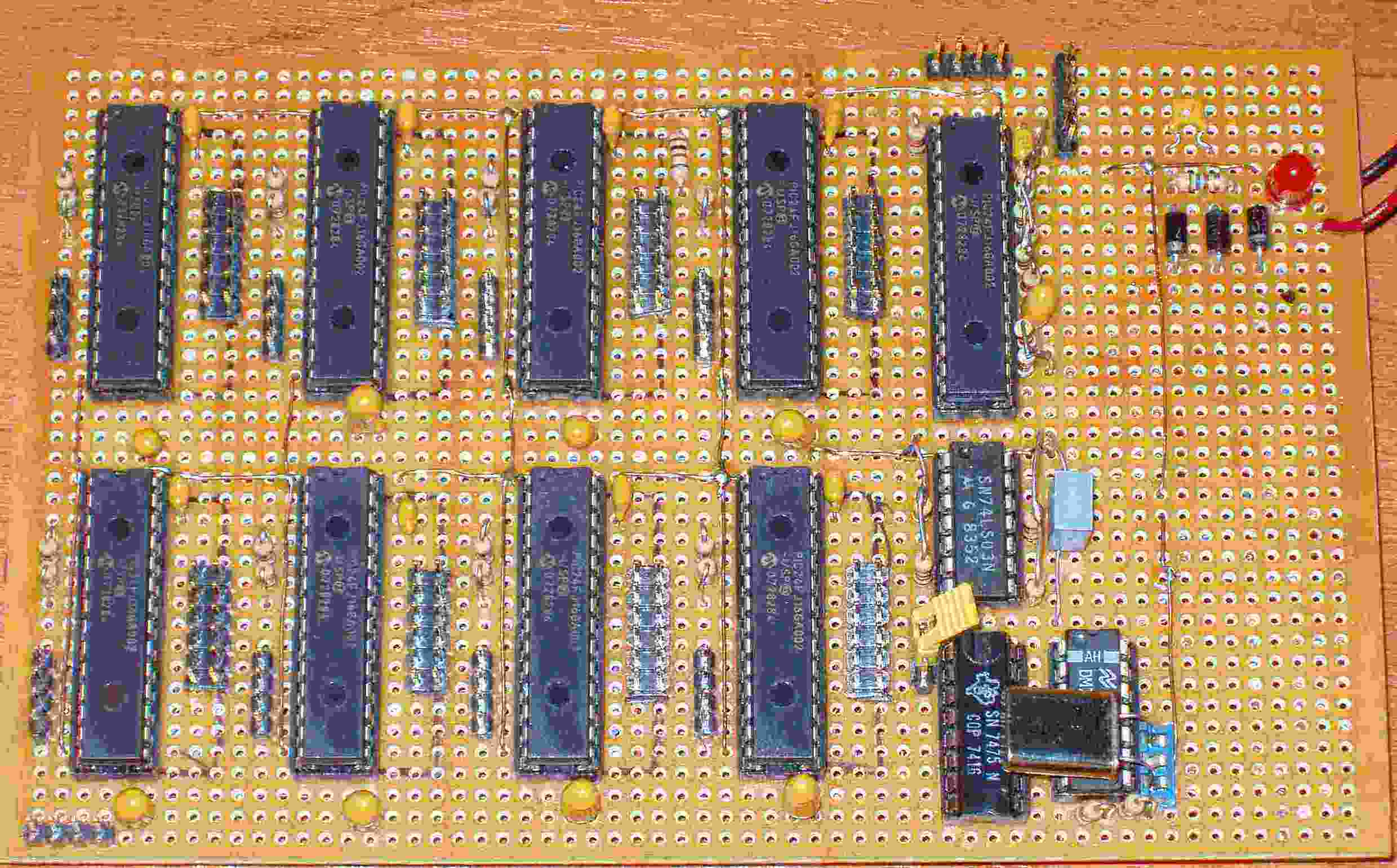
Photograph 1: The prototype of the parallel computer with 8 MCUs.
4. Supporting software
4.1) PC software
The programs that run on the parallel machine are written and assembled using the MPLAB IDE 8.10. They are written in assembly language to ensure the synchronization of the MCUs.
The code is downloaded to the MCUs using the special program that has been developed for this task. The software communicates with the Parallel_PIC machine through the RS232 port (COM1). The software has been developed with Visual Basic 2005 Express Edition (free downloadable from Microsoft). I suggest to create a new project and replace the files "form1.vb" and "form1.designer.vb" with the respective files you downloaded from my site.
The next picture shows an instance of the User’s Interface:
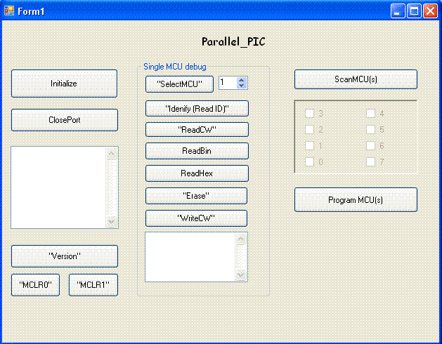
Figure 4: User’s interface of the programming software.
The button "Initialize" is used to initialize the program (it is also done when the program is loaded).
The button "ClosePort" is used to end the communication through the serial port (it is also done when the program is closed).
The button "Version" is used to send the respective command to Parallel_PIC. The result is displayed in the box over this button.
The button "MLCR0" is used to send the respective command to Parallel_PIC. All MCUs enter the RESET state.
The button "MLCR1" is used to send the respective command to Parallel_PIC. All MCUs enter the normal operation state.
At the middle column there are buttons to control a single MCU. They are used mainly for debugging and problem detection on single MCUs, and not on normal operation!
The button "Select MCU" is used in conjunction with the frame on its right to select the MCU that will be referred to on the operations of the other buttons of this column. It sends the respective command to the Parallel_PIC.
The button "Idenify (Read ID)" is used to send the respective command to Parallel_PIC. The result of this command is the ID number of the selected MCU, and is displayed in the frame at the bottom of this column.
The button "ReadCW" is used to send the respective command to Parallel_PIC. The result of this command are the two CodeWord of the selected MCU, and are displayed in the frame at the bottom of this column.
The button "ReadBin" is used to send the respective command to Parallel_PIC. The result of this command is to send the Parallel_PIC all the contents of the Flash memory of the selected MCU. The data transmission is done in binary format. The data are converted to ASCII hex and are stored into file ".\FlashDump.txt".
The button "ReadHex" is used to send the respective command to Parallel_PIC. The result of this command is to send the Parallel_PIC all the contents of the Flash memory of the selected MCU. The data transmission is done in ASCII format. The data are stored into file ".\FlashDumpHex.txt".
The button "Erase" is used to send the respective command to Parallel_PIC. The result of this command is to erase all the contents of the Flash memory of the selected MCU.
The button "WriteCW" is used to send the respective command to Parallel_PIC. The result of this command is to read the two CodeWords of the selected MCU. (Note: the firmware does not still let the user to define the value of the CWs. These values are preset from the firmware.)
The button "ScanMCU(s)" is used to detect the MCUs and to show the available.
The check-boxes are used to select the MCUs that will be programmed.
The button "Program MCU(s)" is used to select the .hex file that will be loaded into all the selected MCUs.
4.2) Firmware
The firmware that run into the "control" MCU is using a serial connection to communicate with the PC. Most of the communication is performed in ASCII formatted commands and their responses. The control MCU executes an infinite loop were it waits for commands from the PC. When it receives a command, the MCU executes it and returns to the mail loop. Although all the commands are formatted in the ASCII code, the data passed travel in binary format in some cases. This means that the software that runs on the PC and communicates with the Parallel_PIC cannot always be a simple ASCII terminal program!
The commands that are implemented include MCU scanning, selecting one of the available MCUS, reading and writing the flash memory of the selected MCU, reading and writing hte Configuration Words of the selected MCU and erasing the flash memory of the selected MCU.
There is a small problem encountered using this software: The flash memory is completely erased in each program cycle. This way the configuration words have to be reprogrammed in each program cycle. So the configuration words are set to their initial state and then reprogrammed for external clock. This procedure “confuses” a little the MCUs. They have to “run” for a while with the external clock and then they operate as expected (which means that the clock can freeze).
5. Parallel programming
Some parallel algorithms will be presented in this section. The code that implements most of these algorithms is not optimized for speed as it has educational purpose. The last example discuses a speed optimized algorithm.
All algorithms use a common initialization of the UART. The UARTs are configured to operate in their maximum baud rate (Fosc / 8). No interrupts are used. The input and output of the UART are mapped to the RPx pins depending on the specific algorithm and topology. This mapping can change during the algorithm execution.
5.1 Linear array – Simple transfer test.
The interconnection network for this algorithm is a linear array of one (1) dimension. This means that all MCUs are considered to form a line. Each MCU communicates with the previous and the next MCU except for the first MCU that has no previous and the last that has no next.
The next figure shows this topology.

Figure 5: A Linear array.
The arcs indicate that the MCUs send data to the right and receive data from the left.
The “problem” is to transfer (or “route”) data from the leftmost MCU (1) to the rightmost MCU (8).
The “solution” follows:
- Each MCU has a variable that holds the data to be propagated.
- Each one of the inner MCUs (2 to 7) transmits the value of its variable to its right MCU and receives a new value for the variable from its left MCU.
- The leftmost MCU reads a new value from PortA instead of reading it from another MCU. For practical reasons this is a 2-bit value from PortA(0,1).
- The rightmost MCU writes its variable’s value to PortA(3,4) instead of sending it to its right.
The code for these three cases is shown in the next table.
;Left loop: ;============ ; read value MOV PORTA,W1 AND W1,W2,W1 ;============= ; send value MOV W1,U1TXREG ;============= ; Wait MOV #100,W3 loopW: NOP DEC W3,W3 BRA NZ,loopW ;============= ; receive value MOV U1RXREG,W1 ;============= ; NOP NOP NOP ;============= BRA loop |
;Middle loop: ;============ ; NOP NOP ;============= ; send value MOV W1,U1TXREG ;============= ; Wait MOV #100,W3 loopW: NOP DEC W3,W3 BRA NZ,loopW ;============= ; receive value MOV U1RXREG,W1 ;============= ; NOP NOP NOP ;============= BRA loop |
;Right loop: ;============ ; NOP NOP ;============= ; send value MOV W1,U1TXREG ;============= ; Wait MOV #100,W3 loopW: NOP DEC W3,W3 BRA NZ,loopW ;============= ; receive value MOV U1RXREG,W1 ;============= ; Write value AND W1,W2,W1 SL W1,#3,W1 MOV W1,PORTA ;============= BRA loop |
Table 1: The code for the simple data transfer on a linear array
The delay between transmission and reception operations is inserted to ensure the correct communication between the MCUs. The delay does not correspond to the exact number of cycles required, but it gives enough time for the UARTs to transmit and receive an 8-bit value.
All MCUs have exactly the same initialization code.
In this algorithm each MCU uses one (1) UART. The receiver of the UART is mapped to pin RP14, while the transmitter is mapped to RP15. The interconnection network is formed by connecting the RP15 of MCU numbered (k) to the RP14 of MCU (k+1).
The NOP lines are inserted to keep synchronization of all MCUs.
The first few data outputted at PortA of MCU 8 have no meaning, as they reflect the values of the variables inside the MCUs. The loop has to be executed seven (7) times to output the correct input. Any change in the input data will be transferred to the output in seven (7) loop executions.
A simple test to ensure the correct operation of the clock “freeze” function is to stop the clock, change the input and see that the output does not change! When the clock is re-enabled, the output changes again. (Remember here that the start-up operation for the parallel computer is described in section 2).
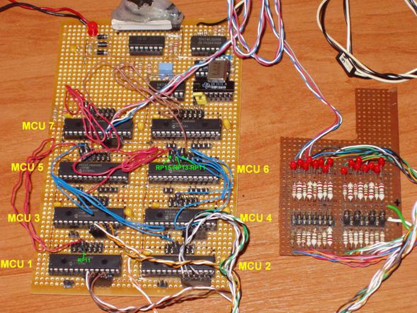
The next photograph shows the parallel computer (the first version of it V1.0) with this topology and a simple test board with jumpers for input and leds for output.

Photograph 2: The parallel computer (V1.0) configured as a linear array.
The project is stored into folder “LinearArray_route”. The source file “LinearArray_route.s” holds the assembly code for the left MCU. When the project is built, the hex file produced must be manually renamed (this is already done and the resulting file is “LinearArray_route_L.hex”). Then the user must replace the code that is specific to the left MCU with the code that is specific for the middle MCUs (a simple copy-paste operation) and rebuild the project. The new hex file is renamed to “LineArray_route_M.hex”. The procedure is repeated once more for the right MCU (file “LinearArray_route_R.hex”). Now the user can use the programmer to store the code to the MCUs. In section 5.3 the use of conditional assembling improves this procedure.
5.2 Tree – Sum of small integers.
The interconnection network for this algorithm is a binary tree with 4 leaves.
The next figure shows this topology.
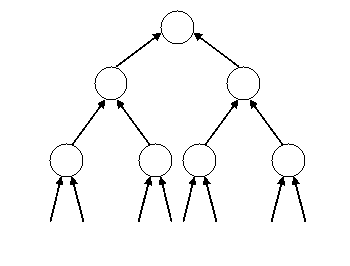
Figure 6: Binary tree with 4 leaves.
The arcs indicate the direction of the data transfers. MCUs 1,2,3,4 are called “leaves”, MCU 5 is the “parent” of MCUs 1,2, so MCUs 1,2 are the “children” of MCU 5. The same naming holds for the other MCUs. MCU 7 is also called the “root” of the tree.
The “problem” is to sum the data that are presented at the inputs of the leaves. The result is outputted from the root.
The “solution” follows:
- Each leaf reads the data from port A. For practical reasons this is a 2-bit value from PortA(0,1). It then transmits this value to its parent.
- Each of the middle MCUs reads the values from its left and right child. It then sums these two values and transmits the result to its parent. (This can be performed for many levels of the tree if the tree has more MCUs.)
- The root MCU performs all the operations of a middle MCU (except for the transmission) and also outputs the result to portA (0,1,3,4). Note that there are 4 numbers summed each one of 2-bits, so the result requires 4-bits for correct representation.
The code for these three cases (leaf, middle, root) is shown in the next table.
;Root loop: ;================= ; read-write value AND W3,W4,W6 SL W3,#1,W7 AND W7,W5,W7 IOR W6,W7,W7 MOV W7,PORTA ;================= ; RxD --> RP15 MOV #0x0008,W6 MOV W6,U1MODE MOV #0x1F0F,W6 MOV W6,RPINR18 MOV #0x8008,W6 MOV W6,U1MODE MOV #0x04C0,W6 MOV W6,U1STA ;================= NOP ;================= MOV #100,W8 loopW1: NOP DEC W8,W8 BRA NZ,loopW1 ;================= ; read left data (W1) MOV U1RXREG,W1 ;================= ; RxD --> RP13 MOV #0x0008,W6 MOV W6,U1MODE MOV #0x1F0D,W6 MOV W6,RPINR18 MOV #0x8008,W6 MOV W6,U1MODE MOV #0x04C0,W6 MOV W6,U1STA ;================= NOP ;================= MOV #100,W8 loopW2: NOP DEC W8,W8 BRA NZ,loopW2 ;================= ; read right data (W2) MOV U1RXREG,W2 ;================= ADD W1,W2,W3 ;================= BRA loop |
;Middle L loop: ;================= ; read-write value NOP NOP NOP NOP NOP ;================= ; RxD --> RP15 MOV #0x0008,W6 MOV W6,U1MODE MOV #0x1F0F,W6 MOV W6,RPINR18 MOV #0x8008,W6 MOV W6,U1MODE MOV #0x04C0,W6 MOV W6,U1STA ;================= MOV W3,U1TXREG ;================= MOV #100,W8 loopW1: NOP DEC W8,W8 BRA NZ,loopW1 ;================= ; read left data (W1) MOV U1RXREG,W1 ;================= ; RxD --> RP13 MOV #0x0008,W6 MOV W6,U1MODE MOV #0x1F0D,W6 MOV W6,RPINR18 MOV #0x8008,W6 MOV W6,U1MODE MOV #0x04C0,W6 MOV W6,U1STA ;================= NOP ;================= MOV #100,W8 loopW2: NOP DEC W8,W8 BRA NZ,loopW2 ;================= ; read right data (W2) MOV U1RXREG,W2 ;================= ADD W1,W2,W3 ;================= BRA loop |
;Middle R loop: ;================= ; read-write value NOP NOP NOP NOP NOP ;================= ; RxD --> RP15 MOV #0x0008,W6 MOV W6,U1MODE MOV #0x1F0F,W6 MOV W6,RPINR18 MOV #0x8008,W6 MOV W6,U1MODE MOV #0x04C0,W6 MOV W6,U1STA ;================= NOP ;================= MOV #100,W8 loopW1: NOP DEC W8,W8 BRA NZ,loopW1 ;================= ; read left data (W1) MOV U1RXREG,W1 ;================= ; RxD --> RP13 MOV #0x0008,W6 MOV W6,U1MODE MOV #0x1F0D,W6 MOV W6,RPINR18 MOV #0x8008,W6 MOV W6,U1MODE MOV #0x04C0,W6 MOV W6,U1STA ;================= MOV W3,U1TXREG ;================= MOV #100,W8 loopW2: NOP DEC W8,W8 BRA NZ,loopW2 ;================= ; read right data (W2) MOV U1RXREG,W2 ;================= ADD W1,W2,W3 ;================= BRA loop |
;Leaf L loop: ;================= ; read-write value MOV PORTA,W1 AND W1,W4,W1 NOP NOP NOP ;================= ; RxD --> RP15 MOV #0x0008,W6 MOV W6,U1MODE MOV #0x1F0F,W6 MOV W6,RPINR18 MOV #0x8008,W6 MOV W6,U1MODE MOV #0x04C0,W6 MOV W6,U1STA ;================= MOV W1,U1TXREG ;================= MOV #100,W8 loopW1: NOP DEC W8,W8 BRA NZ,loopW1 ;================= ; read left data (W1) NOP ;================= ; RxD --> RP13 MOV #0x0008,W6 MOV W6,U1MODE MOV #0x1F0D,W6 MOV W6,RPINR18 MOV #0x8008,W6 MOV W6,U1MODE MOV #0x04C0,W6 MOV W6,U1STA ;================= NOP ;================= MOV #100,W8 loopW2: NOP DEC W8,W8 BRA NZ,loopW2 ;================= ; read right data (W2) NOP ;================= NOP ;================= BRA loop |
;Leaf R loop: ;================= ; read-write value MOV PORTA,W2 AND W2,W4,W2 NOP NOP NOP ;================= ; RxD --> RP15 MOV #0x0008,W6 MOV W6,U1MODE MOV #0x1F0F,W6 MOV W6,RPINR18 MOV #0x8008,W6 MOV W6,U1MODE MOV #0x04C0,W6 MOV W6,U1STA ;================= NOP ;================= MOV #100,W8 loopW1: NOP DEC W8,W8 BRA NZ,loopW1 ;================= ; read left data (W1) NOP ;================= ; RxD --> RP13 MOV #0x0008,W6 MOV W6,U1MODE MOV #0x1F0D,W6 MOV W6,RPINR18 MOV #0x8008,W6 MOV W6,U1MODE MOV #0x04C0,W6 MOV W6,U1STA ;================= MOV W2,U1TXREG ;================= MOV #100,W8 loopW2: NOP DEC W8,W8 BRA NZ,loopW2 ;================= ; read right data (W2) NOP ;================= NOP ;================= BRA loop |
Table 2: The code for the tree-sum algorithm.
The delay between transmission and reception operations has been discussed in the previous algorithm.
All MCUs have exactly the same initialization code except for the portA initialization (the leaves require 2 bits input, while the root requires 4-bit output).
In this algorithm each MCU uses one (1) UART. The transmitter is mapped to RP11. The receiver is connected first to RP15 (in order to read the value from the left child) and then to RP13 (in order to read the value from the right child). This means that the MCU at the left must transmit its value in the first step, and the MCU at the right must transmit its value in a second step. This is reflected at the L and R column for the leaves and the middle MCUs. The difference in the L and R code is in the instance that the data are transmitted.
The interconnection network is formed by connecting the RP11 of the L - MCUs to the RP15 of its respective parent, and the RP11 of the R – MCUs to the RP13 of its respective parent.
The NOP lines are inserted to keep synchronization of all MCUs.
The first few data outputted at PortA of MCU 7 have no meaning, as they reflect the values of the variables inside the MCUs. The loop has to be executed three (3) times to output the correct input. Any change in the input data will be transferred to the output in three (3) loop executions.
The code can be written in a different way where two (2) UARTs are used for the reception of values. This way the whole process is accelerated as the values can be received from both children at the same time, and also no pin mapping reconfiguration is required. However the dynamic pin remapping will be necessary for networks where some MCUs have to transmit or receive data from three (3) or more MCUs. So this is a good example of how this task can be accomplished.
The next photograph shows the parallel computer (the first version of it V1.0) with this topology and a simple test board with jumpers for input and leds for output.
Photograph 3: The parallel computer (V1.0) configured as a tree.
The project is stored into folder “Treesum”. The source file “Treesum.s” holds the assembly code for MCU 1. When the project is built, the hex file produced must be manually renamed (as in the previous example). The resulting hex files are: “Treesum_leaf_L.hex”, “Treesum_leaf_R.hex”, “Treesum_middle_L.hex”, “Treesum_middle_R.hex”, “Treesum_root.hex”.
5.3 Linear array – Sorting.
In another page there is described an algorithm for sorting on a linear array (I/O in each Processing Element).
An improvement can be achieved if the transmitter and the receiver of the UART are used concurrently. This way all MCUs perform compare-exchange operation and there is no need for a second transmission. The next table shows a part of this solution (although not tested yet).
;Odd_L

….

setup_RxD_RP12
;=================
; send data
MOV	W1,U1TXREG
;=================
wait
;=================
; receive data
MOV	U1RXREG,W2
;=================
; compare-exchange
CP	W1,W2
BRA	LE,labA
MOV	W2,W1
BRA	labB
labA:
NOP
NOP
labB :
;=================
NOP
NOP
NOP
NOP
NOP
NOP
NOP
NOP
;=================
; send data
NOP
;=================
wait
;=================
; receive data
NOP
;=================
; compare-exchange
NOP
NOP
NOP
NOP
NOP


;=================

DEC W7,W7
….
|
;Odd_M …. setup_RxD_RP12 ;================= ; send data MOV W1,U1TXREG ;================= wait ;================= ; receive data MOV U1RXREG,W2 ;================= ; compare-exchange CP W1,W2 BRA LE,labA MOV W2,W1 BRA labB labA: NOP NOP labB : ;================= setup_RxD_RP14 ;================= ; send data MOV W1,U1TXREG ;================= wait ;================= ; receive data MOV U1RXREG,W2 ;================= ; compare-exchange CP W2,W1 BRA LE,labAA MOV W2,W1 BRA labBB labAA: NOP NOP labBB: ;================= DEC W7,W7 …. |
;Even_M …. setup_RxD_RP14 ;================= ; send data MOV W1,U1TXREG ;================= wait ;================= ; receive data MOV U1RXREG,W2 ;================= ; compare-exchange CP W2,W1 BRA LE,labA MOV W2,W1 BRA labB labA: NOP NOP labB : ;================= setup_RxD_RP12 ;================= ; send data MOV W1,U1TXREG ;================= wait ;================= ; receive data MOV U1RXREG,W2 ;================= ; compare-exchange CP W1,W2 BRA LE,labAA MOV W2,W1 BRA labBB labAA: NOP NOP labBB : ;================= DEC W7,W7 …. |
;Even_R …. setup_RxD_RP14 ;================= ; send data MOV W1,U1TXREG ;================= wait ;================= ; receive data MOV U1RXREG,W2 ;================= ; compare-exchange CP W2,W1 BRA LE,labA MOV W2,W1 BRA labB labA: NOP NOP labB : ;================= NOP NOP NOP NOP NOP NOP NOP NOP ;================= ; send data NOP ;================= wait ;================= ; receive data NOP ;================= ; compare-exchange NOP NOP NOP NOP NOP ;================= DEC W7,W7 …. |
Table 4: Another solution for the sorting algorithm (not tested).
5.4 Linear array – FIR filter.
The algorithms described so far have a pure educational nature: no one uses 8 MCUs to perform sorting or summing! These “educational” algorithms show that the typical solution involves some steps of communication that alternate with steps of computation. In the previous examples the communication steps have been proven to be slow (there is a “wait” function between each transmission and its respective reception). This “idle” time can be used for computations.
The present example will show the design of an algorithm that can be efficient and practical. The code is not complete and not tested yet.
The “problem” is to perform the computations of a FIR (Finite Impulse Response) filter. This is expressed with equation:
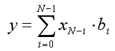
where “y” is the output value, “xi” are the input values, and “bi” are the filter’s coefficients (or taps).
The interconnection network for this algorithm is a linear array of one (1) dimension as in the first example.
The “solution” follows:
- Each MCU holds a set of coefficients and the respective input values. For example, each MCU can hold 64 coefficients, leading to a FIR filter with 8X64=512 taps.
- Each MCU calculates the sum of products for the values it holds.
- Each MCU communicates with the MCU on its right to send the partial result and one of the input values. This way the input values “travel” through the MCUs.
- Each MCU adds the partial result received from its left MCU to its internal partial result before it transmits it to the MCU at its right. (The leftmost MCU assumes zero for input, the rightmost MCU does not have to transmit the input data value but only the result that is now the final result).
- The data values are 16-bits wide and the sums are 32 bits wide.
- The external clock is a multiple of the data input/output rate (an external PLL can be used).
The time between the transmission and the reception can be used for the calculations that do not depend on the received values. This way the communication overhead is minimized as it is restricted to the commands that read/write the UART registers. Of course, having 6 bytes for communication in each loop, there must be enough work for the MCUs to keep them busy during the communication phase. This means that this parallel filter will be efficient only when the filter’s length (i.e. the number of taps) is quite big. But this is the case that requires the use of a parallel machine!
6. Conclusions
This project describes the implementation of a parallel computer that uses the PIC24FJ16GA002-I/SP as the basic processing element. The microcontrollers use their UARTs to communicate. The user builds an interconnection network between the microcontrollers. The Peripheral Pin Select feature is used to dynamically map the UARTs to the desired pins of the microcontrollers. All the microcontrollers execute their code in complete synchronization.
This parallel machine can be used for educational reasons as well as for solving computational intensive problem that can not be solved with a simple microcontroller. The development of the code that is executed is not a simple task as the parallel algorithms are more complicated than the usual algorithms. Some examples are presented to demonstrate the use of this parallel computer.
The prototype consists of eight (8) microcontrollers. However the communication capabilities allow the construction of much greater machines, for example one can build a hypercube of 4096 (=2^12) elements.
The downloading of the code to the microcontrollers is performed with the use of a PC that runs a special program that provides the Graphical User Interface.
Main page of Parallel Processing