Introduction
The term "polarization" (bias) we mean the appropriate constant (dc) voltage (or voltages) to be implement in an electronic circuit element, a transistor and thus to ensure the smooth operation of the continuum, but in the case that would have applied alternating signal to the input of the circuit.
The continuous trend (or trends) determines the polarization resistance value which is achieved through the proper polarization
if known currents. In practice, however, usually work in reverse. We are given that the trends and sources of resistance available and seek to find the polarization currents in the circuit, and trends or pertain to contacts (channels) of the transistor.
1.2 polarizing circuit wiring CE
In connection common-emitter (CE), the emitter is common to the circuit input and output. A polarizing circuit wiring CE shown in Figure 1.1. In this circuit, we want to compute the bias voltages VBE and VCE required for proper operation and resting point Q, around which the operation.
.
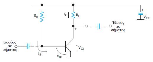
Figure 1.1. Constant polarizing circuit wiring CE
The transistors are NPN type but the following analysis applies to PNP, it is sufficient to reverse the polarities of voltages and direction of currents. For analysis, we consider the whole circuit Sch.1.1 consists of the input circuit and output circuit, so that we can analyze them separately.
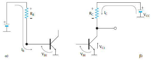
Sch.1.2 depicted in the input and output circuits, which constitute the entire circuit Sch.1.1.
1.2.1 Analysis of the Input Circuit
For the input circuit, Sch.1.2a, law trends Kirchhoff (NTK) gives:

Solving for IB we have
Because VBE is very small compared to the VCC, the nearest we can write:
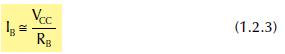
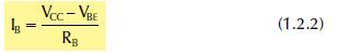
From this relationship, when we know the VCC and RB, we find the ΙΒ.
1.2.2 Analysis of output circuit
Especially for the bias circuits, we can easily assume IE ~ = IC, since we in dc ~ a0 = 1. As we know for hybrid parameters, IC and IB currents associated with the relation:
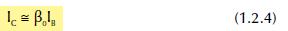
To B0 (static b or b in dc) coincides with the hybrid parameter hFE (while in the second ac coincides with hfe).
Because B0 is known for that particular transistor, and the IB, it follows that, according to Eq. (1.2.4), we can calculate and IC, which is indeed independent of the RC.
From the output circuit, using the NTK, we have also:
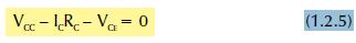

From this relation we determine the polarization voltage VCE, since other sizes of Eq. (1.2.6) is known.
Therefore, the above analysis allows us to identify currents and voltages of polarization.
1.2.3 Point and Direct Load Operation
We consider the typical output of the CE terminal for a typical transistor. The characteristic they seem to Sch.1.3.
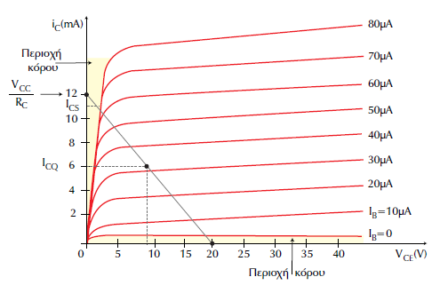
Figure 1.3. Characteristic diagram of CE and direct load
To draw a straight load, we consider Eq. (1.2.6) and solve to IC:
This equation, a diagram with axes VCE ® x and Ic ® y e is a linear relationship of the form
y = mx + l and therefore represents a straight line. The straight line is called the constant load (dc load line).
To draw the load line above, we must identify the two points of a point and slope, which is equal to:

As such points usually take the points of intersection of the axes. So, on one point we and IC = 0 VCE = VCC. So with the known VCC, fixed in one spot. For the other point we consider VCE = 0 thus follows:
IC = VCC / RC
Thus, the RC known, the other fixed point. The final formulation of the direct burdens appear to Sch.1.3.
By drawing the line load, we can determine the operating point or resting Q. To find the Q need to know the price of IB. The value given by Eq. (1.2.3) and suppose that has a value eg IB = 40 μA, just shows Sch.1.3. The intersection of the straight load with the characteristic corresponding to the current base, determines the resting point Q. (Note that during the operation in ac, the operating point back and forth over the so-called ac load line).
1.2.4 Current Korou the transistor
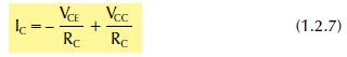
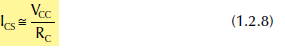
For normal operation of a transistor without the risk of destruction, and in addition to faithful performance of the input signal at the output (ie, without introducing distortion) should the collector current IC is not too large, ie not exceeding a maximum price ICS. The maximum collector current IC is by Eq. (1.2.7) and are:
Το ρεύμα αυτό επιτυγχάνεται, όταν:

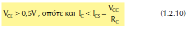
This current, called the saturation current of the transistor corresponds to the upper extremity of the direct burdens (shaded area). For a similar reason, the voltage VCES, which reached the stream, called the saturation voltage. In practice, the VCES, is of the order of a few tenths of a volt.
When the IC is too big, contact the collector of the transistor to overheat and destroy the transistor. Also, if the circuit works as an amplifier, when the IC is very large, we have a faithful reproduction of the input signal at the output. That is, we signal distortion at the output. This is mainly because the circuit is working in non-linear parts of curves Sch.1.3.
So for optimal function, ie to have a linear region, should
into force approach:
1.2.5 Pruning Power Transistors
Based on Eq. (1.2.4), to cut off one transistor, ie to make the collector current IC 0, will be (approximately) zero and the IB. This current IB (~ = 0), for which IC = 0 is called the cutoff current of the transistor.
The Eq. (1.2.4), however, and is roughly in line when the IB become zero, the IC is not exactly zero, and vice versa. It turns out that the exact expression of Eq. (1.2.4) is:
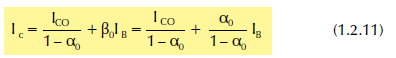
The size of ICO is a new parameter called the transistor and reverse current saturation. This current is defined as the current flowing from the collector at the base of the transistor, when the input is open, ie O = 0 in connection CB. For this reason, the current ICO denoted with the ICBO. The Sch.1.4 shows that the stream is set.
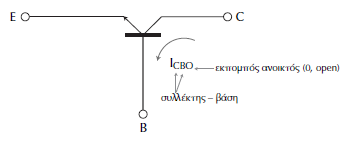
Figure 1.4. Reverse current saturation
To ICO, as a parameter of the transistor is given in the data manufacturers and the transistor is very small. Moreover, by Eq. (1.2.1) we find that we have to cut, ie, IC = 0 we must have IB =-ICO / a0 ~ = - IC0. Therefore, the current will be cut in absolute value equal to the ICO, so very small but not zero.
1.2.6 Effect of Temperature on the Polarization
The circuit of constant polarization Sch.1.1 can provide great enjoyment if you worked as an amplifier. But there are difficulties in maintaining stable polarization, eg remain unchanged resting point Q. This is because the IC varies with temperature. Specifically, the IC because it varies with temperature change and the following three sizes, to which it relates:
1. The reverse saturation current, ICO, which is doubled for each increase in temperature of 10 ° C.
2. The voltage base-emitter bias, VBE, which, with increase in temperature of 1 C, reduced by 2.5 mV [see also Eq. (1.2.2) with an increase in IB].
3. B0 The gain of the transistor, which increases with temperature.
O! values of these quantities as a function of temperature for
a standard silicon transistor (Si), are shown in Table 1.2.1.
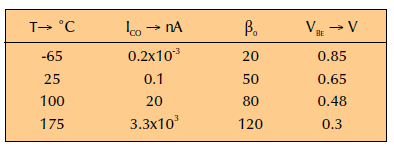
Table 1.2.1. Change of IO,, 0 and VBE, as a function of temperature in Si transistors
Considering the values in Table and Eq. (1.2.11), we conclude that the increase in temperature easily vary the initial conditions of polarization. Specifically, changing the characteristic of the transistor and the collector current IC corresponding to the resting point Q.
To demonstrate the effect brought about by the ICO and B0 polarization conditions when they change with temperature, we consider its characteristic Sch.1.5. Typical were taken at temperatures 25 C and 100 C for the same transistor.
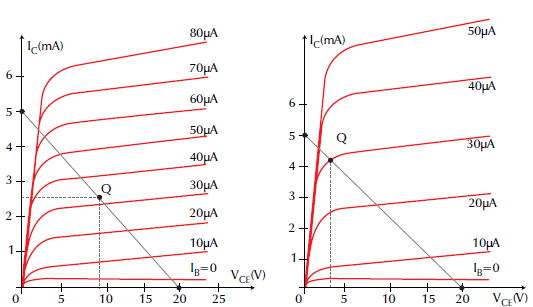
Figure 1.5. Transfer point Q due to change of temperature 25 ° C (a), 100 ° C (b)
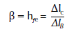
From this figure we see that the rest point Q on the line shifted burden to higher values of IC and even at 1000 C is near saturation. This is because both the ICO, the B0 and increased with temperature. The increase of B0 with temperature, shown by the increase of the characteristic distance along the line load. To certify this, we consider the general definition of the potential b (ie b in ac or hfe) for which we have:
For the same change in the characteristic DIV (a) and (b), the DIC (b) is greater than in (a). In this relationship, this corresponds to an increase in b with temperature, as is shown by Table 1.2.1.
The change in VBE with temperature has much effect on the polarization conditions (eg location of point Q), as the change of B0. We mention only that in order to reduce the effect of VBE bias conditions, often connect a resistor between emitter and RE earth.
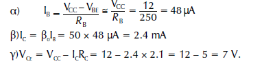
example 1-1
To calculate the voltages and bias currents for the circuit of CE Sch.1.6. The transistors are NPN type and has B0 = 50.
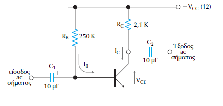
Figure 1.6. Constant polarizing circuit wiring CE
solution
We follow the path previously mentioned, so based on Eq. (1.2.2), (1.2.4) and (1.2.6), we have: