
Circuit CE polarization independent of hfe
As discussed above, current, Ic, and the polarization conditions generally change when the temperature change, because change mainly, CO, VBE and vo. But with modern construction techniques of transistors has been achieved, so the parameter, CO, is minimal. In this way, even at higher temperatures (~ 1000 C), can be seen that, CO has little effect on the initial conditions of polarization. Moreover, as already said, the bias voltage VBE can become independent of temperature, if the emitter is grounded through the emitter resistor RE. Therefore, vo is the size that is substantially alter the conditions of polarization, when the price changed. The vo is known to increase with temperature, but even for transistors that are registered with the same number of lists can be quite different. (It is noted that transistors with the same number
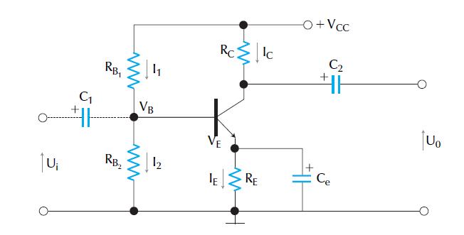
Figure 1.7. Biasing circuit is independent of B0 (wiring CE)
17
registration may have from 125-300 B0 at the same temperature.
Especially for silicon transistors, the B0 shows the temperature changes greater than in germanium transistors. To reduce the effect of B0 on polarization conditions, when the temperature changes the transistor replaced the use of the circuit Sch.1.7. The resistors RB1 and RB2 form a voltage divider and therefore the
voltage VB is given by:
If now the VE represents the voltage across the RE and the VBE voltage between the emitter-base, we get:
The current IE calculated from this trend, as follows:
Since Ib = ~ 0, it follows that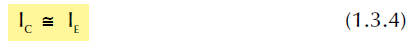
The voltage at the ends of VRc RC will be: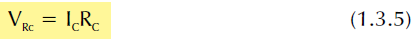
The voltage between collector-ground will be:
The voltage VCE between the collector-emitter will be:

18
Throughout the previous analysis was not used anywhere in B0. So, this bias circuit is practically independent of B0 and the transistor temperature changes, which do not affect either the VB or the VE. As we have seen, the base voltage VB only determined by the RB1, RB2 and the voltage VCC. Also, the emitter voltage VE is stable, because the VB is constant and approximately equal to, since VB >> VBE, with VBE~=0.3 V (Ge) and VBE ~= 0.7 V (Si).
The RE determines the resistance values of the currents IE and IC. Finally, the RC determines the resistance of the collector voltage VC and hence the bias voltage collector-emitter VCE.
The base voltage VB of the adjusted RB2, the collector current IC of the RE and the collector-emitter voltage of the RC. Change any other element of the circuit, will have little effect on the initial conditions of polarization. O capacitor CE is an active part of the circuit when the circuit works as an amplifier, ie an alternating signal at the entrance. However, its presence does not alter the polarization.
The circuit described circuit called polarization voltage divider is the most common in practical applications.
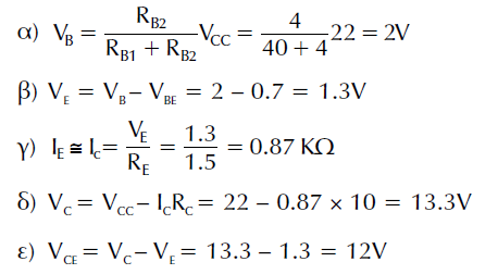
example 1-2
To calculate the voltages and currents in the bias circuit Sch.1.8 if the transistor is silicon.
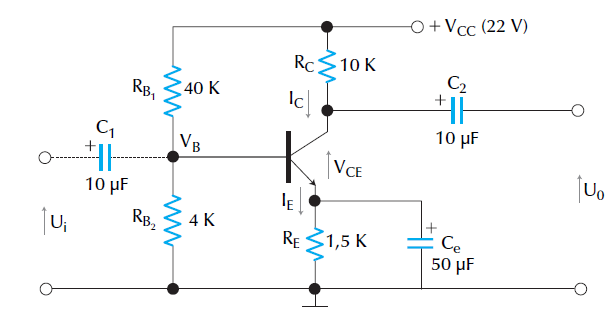
Figure 1.8. Bias circuit with a voltage divider CE
solution
From Eq. (1.3.1) to (1.3.8) take the following order:
19
CE 1.3.1 Polarization Resistance RE
Besides the above, another polarizing circuit wiring CE, which is often used, is the circuit CE with RE the emitter resistance, Sch.1.9.
Figure 1.9. CE circuit polarization resistance RE
It turns out that the base current is given by:
20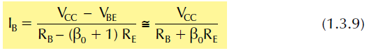
where we make the assumption VBE <
IB shows the current practically independent of VBE.
1.4 Effect of polarization distortion
In practice, the deflection means not faithful performance of the waveform of the input signal at the output of a gradient, eg an amplifier. The term "signal" we mean any variable (basically, AC) voltage, applied to an input amplifier, or take the exit.
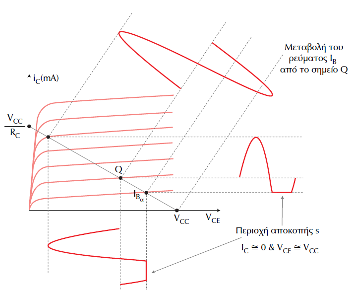
Figure 1.10. Straight load and resting point Q on a typical output BJT
21
There are several reasons why the input signal is not true to the exit. One of the main reasons for failure to obtain appropriate polarized conditions. To be sure the signal will suffer distortion, the initial conditions must be maintained polarization almost unchanged throughout the operation of the amplifier.
For the study of deformation in relation to the polarization, we start with the mathematical expression of the direct connection to load CE, given by Eq. (1.2.7).
If we now assume that the sizes VCC and RC are known, eg VCC = 20 V and Kos RC = 2ΚΩ, then the load line drawn on the diagram of a typical transistor characteristics as shown in Sch.1.10.
As discussed in paragraph 1.2.3, to find the point of resting Q, defined as the central point around which performs the function of the amplifier, you must calculate the base current IB bias. This current is found by Eq. (1.2.3). So if, for optimum operating conditions, we want to point Q is calm in the middle of the line load, we must choose the RB,
so that: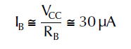
The intersection of the given load directly to the characteristic corresponding to ΙΒ = 30 μA determine where tranquility Q. H VCE voltage corresponding to the point of calm serenity called voltage and collector-emitter is often symbolized by VCEQ. Similarly, the bias current of the collector is denoted ICQ, as shown in Sch.1.10.
If now the input of the amplifier, the amplifier specifically Sch.1.6, apply a signal, the instantaneous voltage VCE will vary around the resting voltage VCEQ. But with the change of the VCE, and will change the instantaneous collector current IC around the stable
price of ICQ.
If the point Q is selected in the middle of the line load and the input signal is small, fluctuations of VCE will not exceed the maximum value, ie the voltage VCC, nor the minimum, ie, VCE = VCES ~ = 0. Thus, the corresponding fluctuations around the fixed ICQ will not exceed the minimum IC ~ = 0 and the maximum IC ~ = VCC / RC.
22
At any time the output voltage, ie the voltage across the RC, expressed as the product of the instantaneous power IC for resistance RC. Then the conditions just mentioned, the output voltage will be a faithful performance of the signal input voltage. Therefore, the signal output voltage will be free of distortion.
But if the point Q calm mounted directly to the low volume (small values of ΙΒ) or move down due to a change of polarization of the initial conditions, then, marks the entrance of large amplitude may appear distorted at the output.
To better understand this issue, we consider the graphical method of depicting Sch.1.11.
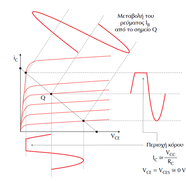
Figure 1.11. Effect of point Q in the resting signal distortion eisodou.To Q is near cutoff.
23
As shown in the figure, the point resting Q is initially placed near cutoff. If the input signal amplitude is large, then the voltage VCE is approximately equal to the voltage VCC, or greater than that, when the output current IC will be approximately zero. Therefore, each instantaneous value of voltage greater than VCC VCE will be cut off (clipped). Thus, the respective IC output throughout this period, maintains constant value of about 0. The complete sinusoidal curve at the top of Sch.1.11, represents the fluctuations of the base current IB from the point of rest, ie: about IBQ.
If we now assume that the Q is placed near saturation (large values of ΙΒ), then, as shown in the graphic chart Sch.1.12, each smaller than the voltage VCE = VCES ~ = 0 will be cut off (clipped).
Therefore, throughout this time period over which the VCE would take prices lower price of approximately zero, the output current is kept constant IC equal to the maximum IC ~ = VCC / RC. That is, the output current
shear has been at level IC ~ = VCC / RC.
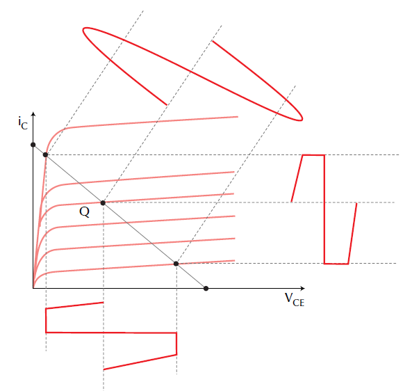
Figure 1.12. Effect of position of point Q in the rest of the input signal distortion. The point is resting near saturation
24
With the above analysis we saw that the site of the resting Q is important for the distortion, which is the input signal. However, even if the Q installed correctly (ie about the middle of the line load), and have the width of the input signal is sufficiently small that the VCE does not exceed the extreme values of VCE ~ = 0 and VCE ~ = VCC. The Sch.1.12 shows the graphical representation method of signal distortion when Q is in the correct position, but the width of the input signal is too large.
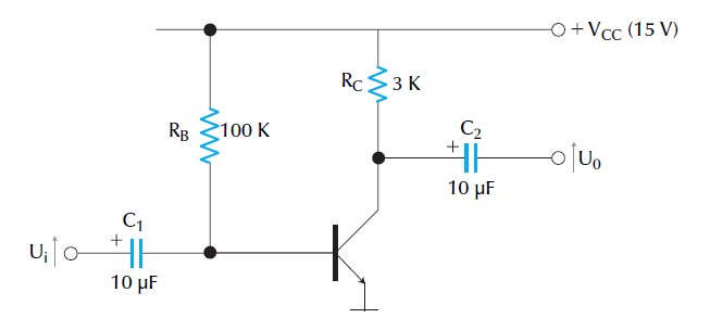
Figure 1.13. Input signal distortion due to overstimulation. Proper placement of the point Q, but with a large input signal
example 1-3
Consider the circuit of Sch.1.14 and typical collector
transistors, Figure 1.15. To calculate:
a) The load line at constant (dc) and the resting point Q.
b) The sizes VCE, IC, VCC / RC and IE corresponding to the resting point Q
(graphical method).
25
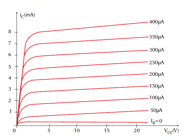
Figure 1.14. Practical fixed bias circuit CE
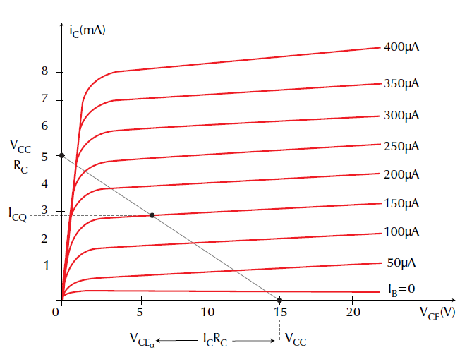
Figure 1.15. Typical collector BJT of Fig 1.14
26
solution
To draw a straight load, we must identify at least two points. One has coordinates:
IC = 0, VCE = VCC = 15 V
and the other,
VCE = 0, Ic = Vcc / RC = 15/3 = 5mA
The straight line joining these points seem to Sch.1.14 and the line is the constant burden for the circuit given.
To determine the resting point Q, must calculate the base current of IB.
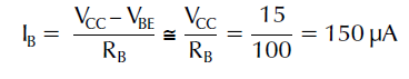
The intersection of the straight load with the characteristic corresponding to IB = 150 μA set point resting Q.
From this figure, we find the required graphics sizes corresponding to point Q.

Comments
I don't know who you are but certainly you are going to a famous blogger if
you aren't already ;) Cheers!
RSS feed for comments to this post